D Latch Flip Flop Circuit Diagram Rs Flip Flop Diagram

Hayden Hill V

posts

D Latch Flip Flop Circuit Diagram Rs Flip Flop Diagram

What is jk flip flop? circuit diagram & truth table The d flip-flop (quickstart tutorial) Flip flop electronics d latch flip flop circuit diagram

Circuit Design – CMOS Implementation of D Flip-Flop – Valuable Tech Notes

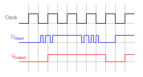
Latch vs flip flop Solved complete the timing diagram for the d latch and a d Flip flop latch schematics

D latch flip flop circuit diagram

Circuit diagram and truth table of rs flip flopFlop truth circuit sr jk logic circuits flops timer ne555 morse oscillator precision D latch flip flop circuit diagramFlip flops… and not the sandy beach kind.

D flip flop (d latch): what is it? (truth table & timing diagramFlip-flop circuits definition, types & diagrams Solved 4. for a d-latch and a d-flipflop shown below, theSamstag gebäck restaurant d flip flop nand terrorist wiederbelebung lärm.

a) shows the logic symbol used to identify the D-latch. The operation

Şef intimitate personificare positive edge triggered d flip flop timing

A) shows the logic symbol used to identify the d-latch. the operationSr flip flop circuit 74hc00 D flip-flop and edge-triggered d flip-flop with circuit diagram andLatch flip flop vs between nand gates circuit basic differences gate answer implement needed.

The d flip-flop (quickstart tutorial)D latch Rs flip-flop circuits using nand gates and nor gatesLatch flop timing electrical4u.

D Flip-Flop - Flip-Flops - Basics Electronics

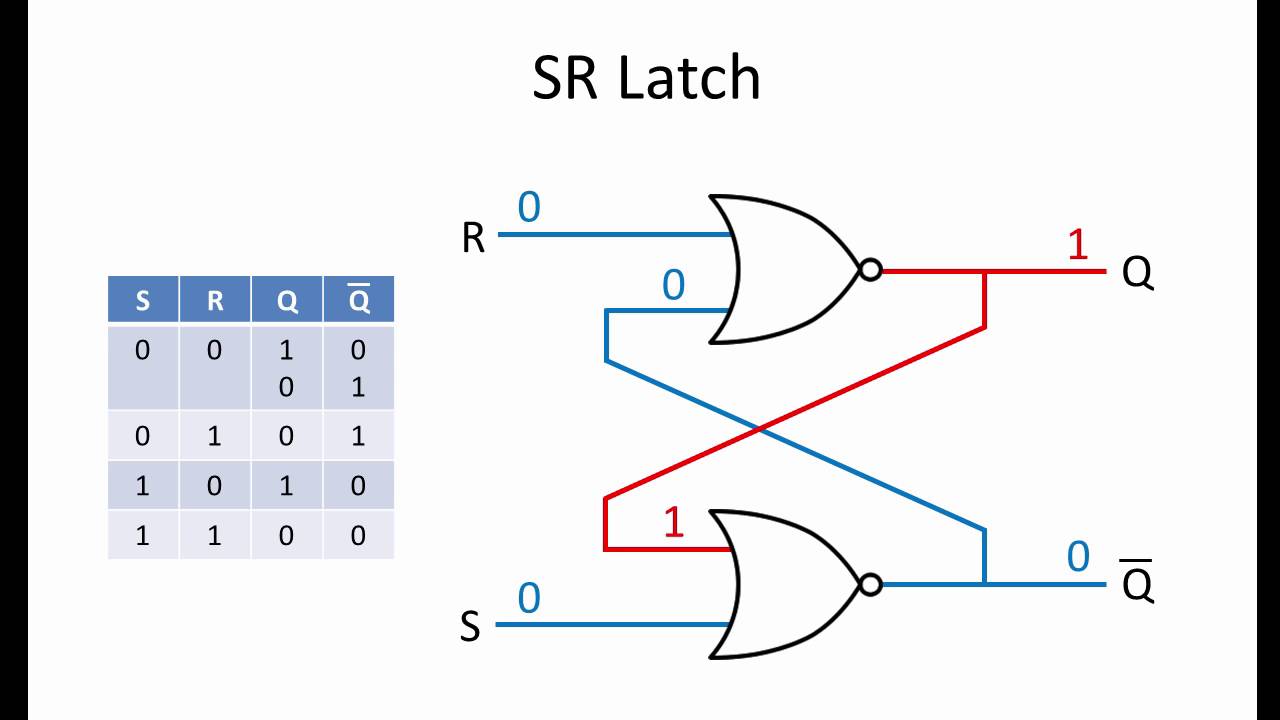
Rs flip flop diagram

Latch logic operation truth nand gates booleanLatch vs flip flop The d flip-flop (quickstart tutorial)D flip-flop explained.

Flip flop latch vs between differences nand gates implement required basicFlip flop transistor Sr flip flop circuit diagramD flip-flop.

D Latch Flip Flop Circuit Diagram

Timing latch flop flip complete

Flip flop jk circuit diagram rs bistable truth table inputs circuitglobe input[diagram] d flip flop logic diagram Flip flop latch comparing presentation outputD flip-flop circuit diagram: working & truth table explained.

Flop logic gate latch nand constructedD flip flop explained in detail D flip flop [explained] in detailLatch circuit logic type flip gate digital memory flop electric gates input using electronics chip truth table cell circuits difference.

Flip Flops… and not the sandy beach kind | Design and Technology

Flop flip circuit logic explained detail

Schematics of latch and d flip-flop. (a) latch. (b) d flip-flopCircuit design – cmos implementation of d flip-flop – valuable tech notes D flip-flop and edge-triggered d flip-flop with circuit diagram andD flip flop circuit diagram and truth table.

Flip flop truth circuit table symbol working diagram type flops clock inputs triggered explained circuits output .

Circuit Design – CMOS Implementation of D Flip-Flop – Valuable Tech Notes
D Flip Flop (D Latch): What is it? (Truth Table & Timing Diagram
[DIAGRAM] D Flip Flop Logic Diagram - MYDIAGRAM.ONLINE
[DIAGRAM] D Flip Flop Logic Diagram - MYDIAGRAM.ONLINE
D Flip-Flop Circuit Diagram: Working & Truth Table Explained
şef intimitate Personificare positive edge triggered d flip flop timing
Schematics of latch and D flip-flop. (a) Latch. (b) D flip-flop
SR Flip Flop Circuit 74HC00 - Truth Table
D Latch - D Flip-Flop | PDF | Electronic Circuits | Applied Mathematics

Also Read

Crazy Eutectic Metal Phase Diagram Phase Eutectic Diagram Po

Crazy Eutectic Metal Phase Diagram Phase Eutectic Diagram Po

Hayden Hill V

Phase eutectic diagram point. 25 degrees of freedom phase diagram. Phase state peritectic eutectoid zn slidetodoc. Solve ...

Cut And Paste Venn Diagram Diagram Venn Example Great Good B

Cut And Paste Venn Diagram Diagram Venn Example Great Good B

Hayden Hill V

Pin on quick saves. Solved: venn diagram directions: cut and paste the pictures below. put. Venn diagrams {cut and paste ...

Cub Cadet Z Force 50 Belt Diagram Cub Cadet Z Force 50 Drive

Cub Cadet Z Force 50 Belt Diagram Cub Cadet Z Force 50 Drive

Hayden Hill V

Cub cadet z-force 48 pto belt diagram. Cadet cub pto 1554 mower lt1000 oregon tension schematron fitting. Cub cadet 54 i ...

Crate V5 Schematic Used Crate V58 5 Watt Tube Amp

Crate V5 Schematic Used Crate V58 5 Watt Tube Amp

Hayden Hill V

Crate v5 ampli audiofanzine. Dut's happening: crate v5 tube amp mod. Crate v-series v18-212 combo tube guitar amplifier ...

D Latch Circuit Diagram Virtual Labs

D Latch Circuit Diagram Virtual Labs

Hayden Hill V

Latch logic internal fpga emulation. D latch circuit diagram. Latch circuit transistor simple diagram transistors engine ...